Industry: Semiconductor
Country: Japan
As semiconductor manufacturing processes continue to evolve, the demand for advanced technologies in die bonding—a critical process in the backend packaging stage—is rapidly increasing. Die bonding requires placing chips onto packaging substrates with extremely high precision, a process that directly affects the performance and reliability of semiconductor devices. As a result, die bonders have become one of the most critical pieces of equipment in the semiconductor packaging process.
Die bonders are responsible for picking up chips from diced wafers and accurately placing them onto the substrate. Using epoxy for bonding, these machines must achieve high-speed and high-precision placement, completing key tasks such as alignment, positioning, flip-chip mounting and sequential bonding. With increasing standards for die bonding accuracy, traditional optical automated inspection systems can no longer meet the micron-level precision and stability requirements. The adoption of precision automated die bonders is now essential, significantly enhancing product yield and production efficiency while reducing human error and providing reliable support for semiconductor manufacturing.
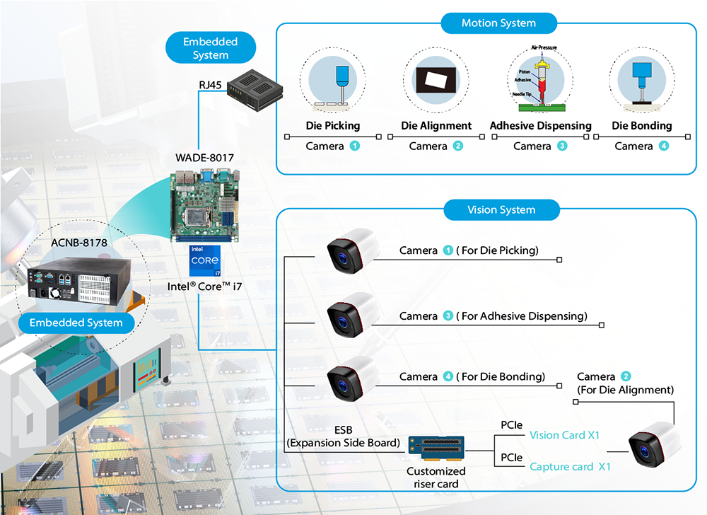
In this project, the customer’s die bonder integrates a motion system and a vision system to achieve ultra-high-speed and precise wafer inspection and positioning. The vision system provides real-time detection of the chip’s position and angle, utilizing image processing algorithms to calculate the relative positions between the chip and the substrate. This data is used to generate compensation values. The motion system dynamically adjusts using the compensation data, ensuring precise alignment and placement of the chip during high-speed pick-and-place operations.
By repeating these operations with extreme precision, the system avoids cumulative errors that could lead to misalignment. Typically, deviations are controlled within micron (μm) levels. Insufficient precision could result in electrical connectivity issues or reduced thermal conductivity, impacting product performance and the overall success of the semiconductor production line. Therefore, the seamless collaboration between the vision and motion systems is crucial for building high-precision die bonders.
Portwell’s customized 4U ACNB-8178 system combined with the WADE-8017 motherboard features 6th and 7th generation Intel® Core™ i3/i5/i7 processors and DDR4 memory. This solution supports high-resolution imaging capabilities for accurate wafer position and orientation detection, enabling robotic arms to swiftly perform pick-and-place operations.
The system’s high-performance computing processes fiducial marks on the substrate for rapid detection, providing compensation data to the motion system to ensure precise chip placement. This significantly improves alignment accuracy and production efficiency, meeting customer demands for die bonders with precision.
The WADE-8017 motherboard is equipped with Intel® I219LM and I211AT Ethernet ports to ensure stable data and image transmission. It supports PCIe x16 Gen3 and six SATA III RAID configurations, enabling efficient data retrieval and storage for chip pick-up, positioning, and measurement.
Portwell’s customized riser cards support high-performance image capture and vision cards, enabling seamless integration with industrial cameras. This ensures real-time alignment and angle correction data for motion control systems, achieving the high-speed and high-precision placement required to bond dozens of chips per second.
The system includes extensive I/O interfaces, such as six COM ports and multiple USB 3.0 and 2.0 ports, providing flexible connectivity for peripheral devices. A custom BIOS enhances system integration and reliability. Additionally, the system supports a 24/7 operational 2.5-inch 500GB hard drive, ensuring stability under high-load, real-time conditions. Optimized thermal designs and a robust architecture guarantee long-term, high-efficiency operations.
Portwell offers end-to-end DMS (Design, Manufacturing and Services), covering standard products and fully customized solutions. Our services include local business communication, FAE technical support, consulting during project execution, after-sales services and root cause analysis for any issues. With a global logistics network and local support in Taiwan, the USA, Japan, China, the UK, Germany, and India, Portwell ensures faster and more effective communication during development and testing, reducing turnaround time to meet customer needs.
Our goal is to deliver value-driven products and superior services that provide a competitive edge for our clients. If you have any inquiry about our products or services, please feel free to contact us. We look forward to assisting you and hearing your feedback!